


Thin Film Circuit Technology hmanga siam a ni
Hrilhfiahna
Technical Parameters 1000 a ni.
Product Hrilhfiahna
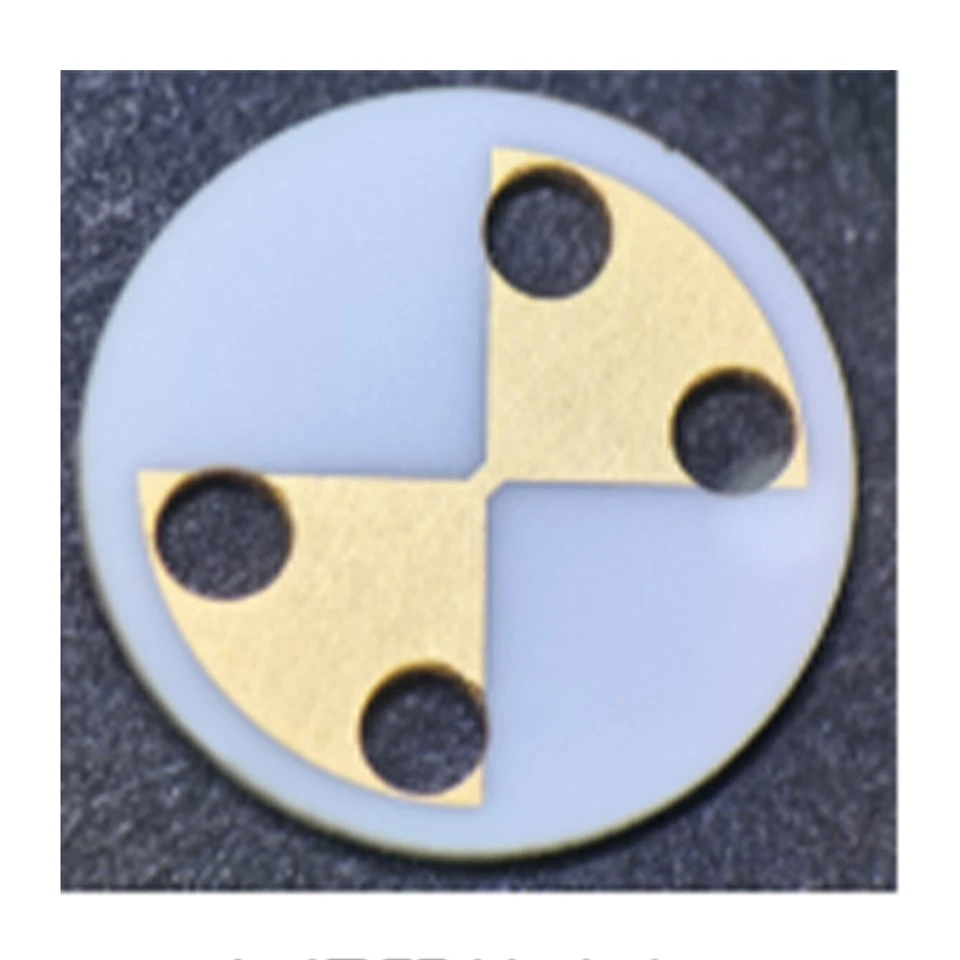
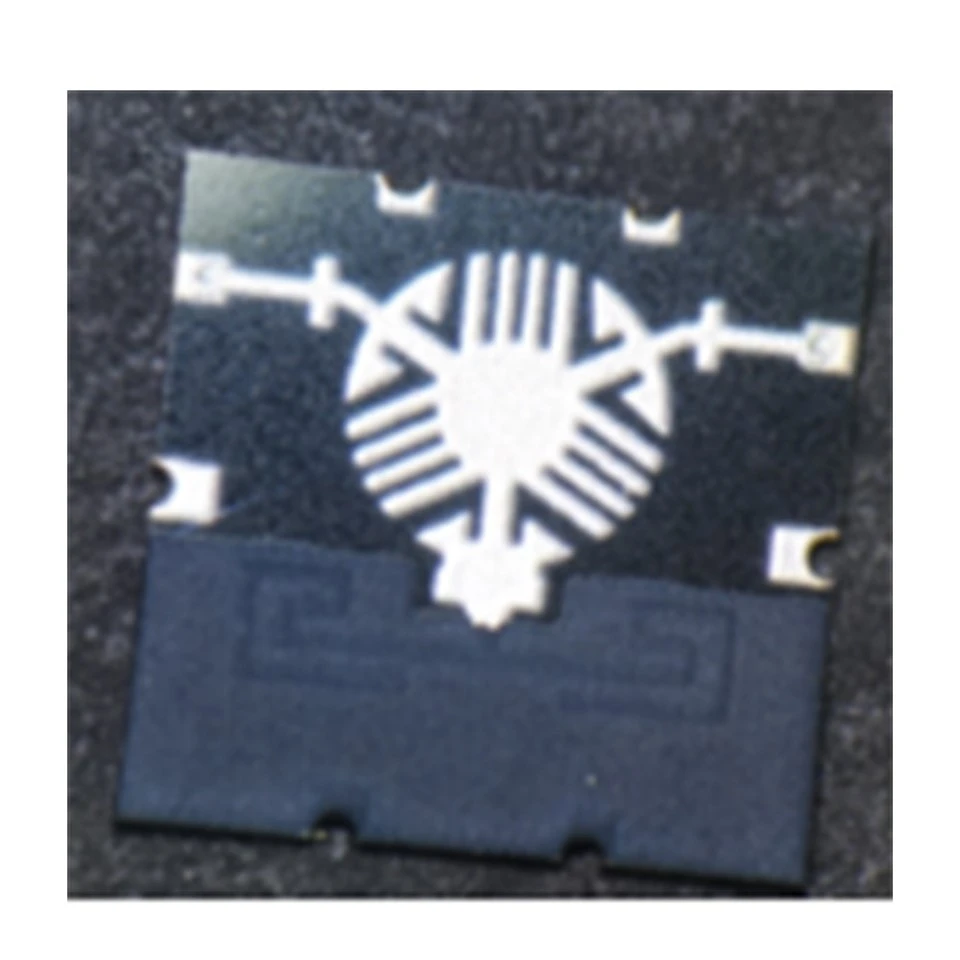
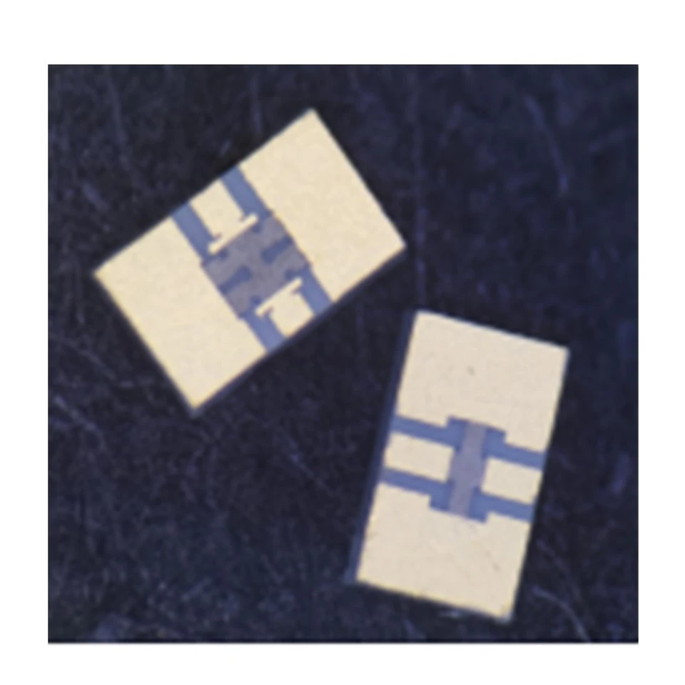
Thin Film Circuit Technology hian thin film deposition, photolithography, etching, leh metallization process hmangin ceramic, glass, emaw silicon-based materials chung lamah micron-scale conductive line a siam a, hei hian high-density, high-reliability electronic integration a siam thei a ni.
Product a thatna te
Linear Precision sang tak nei:Precision photolithography leh vacuum deposition process hmangin standard linewidth leh spacing chu 20μm a thleng thei a, special project-ah chuan 10μm level a thleng thei a ni.
Signal hloh tlem:High-purity metal thin film leh fine line design hian resistance leh transmission loss a ti tlem a, 5G communication, millimeter-wave, leh high-speed electronic system atan a tha hle.
Heat Dissipation tha tak a ni:Thermal conductivity sang tak substrate alumina leh aluminum nitride te nena inzawm chuan heat hi rang takin a bo thei a, device temperature a tihhniam bakah system stability a ti tha hle.
Engvangin nge Thin Film Technology
Integration sang zawk neih a ni
High-density circuit design a support a, product size a tihtlem bawk.
Electrical lama hnathawh dan tha zawk
Signal hloh a tihtlem bakah transmission efficiency a ti tha bawk.
Thermal Management tihchak a ni
Power device hrang hrang tan heat dissipation a ti tha.
Dam rei zawk
Failure rate leh maintenance cost a tihhniam.
Material duhthlan tur
Substrate hmanrua: 1.1.Alumina (Al2O3), Aluminum Nitride (AlN), Silicon Nitride (Si3N4), Glass-Ceramic hmanga siam a ni.
Metal System hrang hrang: 1.1.Rangkachak, Tangkarua, Copper, Nickel, Platinum, leh Custom Multilayer Metal Structure te a awm a.
Technology lama theihna te
Thin Film Deposition-ah hian a awm a:Metal leh functional film hrang hrang siamna kawngah a pui thin.
Lithography dik tak: 1.1.Micron-level circuit patterning a siam thei.
Etching dik tak chu:Circuit dimension leh consistency a enkawl.
Lei chunglam Metallization: 1.1.Gold plating, silver plating, leh ENIG processing te a support bawk.
Multilayer Integration hmanga inzawmna:Single-layer, double-layer, leh multilayer structure design te a support.
Technical lam thil chi hrang hrang
|
Thil |
A sawifiahna |
|
Line zau zawng/Spacing pangngai |
20/20 μm |
|
Thiltihtheihna sang tak nei |
10/10 μm thleng hnuai lam* |
|
Substrate hmanrua te |
Al2O3, AlN, Si3N4, Glass te pawh a awm bawk |
|
Metal System hmanga siam a ni |
Au, Ag, Cu, Ni, Pt |
|
Circuit Layer hrang hrang a awm |
Single / Double / Multilayer a ni |
|
Operating Temperature a ni |
-55℃atanga 300℃thleng a ni |
|
Surface Finish a ni |
ENIG, Rangkachak hnawih, Tangkarua siam |
|
Metallization Thickness a ni |
Customized a ni |
|
Custom Design a ni |
Remchang |
Quality Assurance neih a ni
System tha tak tak enkawl dan
ISO standard angin process control kimchang-.
Raw Material zawn chhuah theihna
Batch enkawl dan leh full-process traceability.
Rintlakna finfiahna
Thermal cycling, damp heat, leh electrical performance testing te a support bawk.
Conformity Control a ni
Hun rei tak-supply stability a enkawl.
Application Industry hrang hrang te
Semiconductor hmanga thil siam chhuah:High-density interconnect leh advanced packaging substrate atan hman thin.
Power Electronics hmanga thil siam:IGBT, SiC, leh power module-ah te hman a ni.
RF Inbiakpawhna: 1.1.5G, millimeter-wave, leh radar system atan a tha.
Automotive Electronics hmanga thil siam chhuah:Energy thar lirthei leh automotive-grade module-a hman thin.
Damdawi lam Electronics: 1.1.High-reliability electronic devices mamawh a tlin.
Aerospace atanga lo chhuak:Temperature sang-temperature leh complex environment application atan a tha.
Customization theihna te
Drawing Customization hmanga siam dan:Gerber leh CAD file siamna a support bawk.
Material Customization hmanga siam dan:Thermal conductivity leh electrical performance mamawh dan atanga material thlan dan.
Structure tihchangtlun dan:Circuit leh multi-layer structure design a support bawk.
Mass Production atanga sample lak tur:One-stop development services a pe thin.
Company chakna
20+ Kum tam tak chhung thil siam chhuah lama tawnhriat nei
Kum 2003-a din niin, R&D leh inorganic thil thar siamna lama tui tak, kum 20 chuang zet industry lama tawnhriat nei tawh a ni.
Production theihna nghet tak neih theihna
Production base lian tak-a nei a, manufacturing system kimchang tak a nei a, global client atanga hun rei tak-stable procurement a thlawp a ni.
Professional R&D Team te an ni
Material R&D leh performance optimization theihna a nei a, customized solutions a pe thei bawk.
Quality Control khauh tak neih a ni
Testing hmanrua hmasawn tak tak hmanga thuam, product quality leh batch stability khauh taka control.
Khawvel pum huapa Export lama tawnhriat nei
Products hi ram pawn market-ah thawnchhuah a ni a, export service puitling tak tak leh customer support theihna neiin a awm bawk.
Customized Solutions te chu a hnuaia mi ang hian a ni
Customer mamawh hrang hrang phuhruk nan product specification, performance, leh application mamawh customization a support.
FAQ
hot tags .: thin film circuit technology, China thin film circuit technology siamtu, supplier, factory
Next2
Thu hriat tur a awm lo .Inquiry thawn rawh .


